Obsidian pillar (of the Blood Temple)
-
Ever wanted an RSS feed of all your favorite gaming news sites? Go check out our new Gaming Headlines feed! Read more about it here.
-
We have made minor adjustments to how the search bar works on ResetEra. You can read about the changes here.
Xbox Series X: A Closer Look at the Technology Powering the Next Generation
- Thread starter Deleted member 5028
- Start date
You are using an out of date browser. It may not display this or other websites correctly.
You should upgrade or use an alternative browser.
You should upgrade or use an alternative browser.
then how would they sell elite controllers?
Didn't they already confirm that this is the case? That there are no "next-gen only" games for like a year or two?Yeah the games they showed was the only thing that let me down, can't expect people to go wow over Halo 5, Gears 5 and Minecraft, even if they're upgraded. They need to show some games before people start thinking this is another X update for Xbox One.
My knowledge does run run that deep anymore, but I know enough that all these specs impress me and surpass some of my expectations. My only (slight!) letdown in the amount of RAM?
Someone who is smarter than me: Thoughts on the RAM situation? I assume now that the XSX is equipped with an NVME SSD it'll use that as a sudo-RAM (Virual RAM) albeit slower, once it allocated all 16GBs? GDDR6 is fairly speedy, correct?
Thanks!!
Give this a quick spin, see "Xbox Velocity Architecture", "Sample Feedback Streaming" and "Direct Storage". Should clear up how they're going about it.
Nice to see that next-gen actually has CPUs fairly equal to current PCs. That was a pretty weak aspect of the current-gen consoles.
Everything looks pretty good though, and I look forward to seeing what the PS5 has to offer since I'm not really interested in Xbox.
16GB of RAM is disappointing though considering how powerful everything else is. 16GB isn't a lot when it's being shared by the entire system.
Everything looks pretty good though, and I look forward to seeing what the PS5 has to offer since I'm not really interested in Xbox.
16GB of RAM is disappointing though considering how powerful everything else is. 16GB isn't a lot when it's being shared by the entire system.
AA batteries > InternalThe biggest disappointment is that AA batteries are still around.
This is coming from a guy who owns the elite 2 controller. If you want a rechargeable battery pack you can buy one.
What is the source for this? Just curious.There's a rumor kicking around that they were looking at September but COVID19 may have pushed that back. We'll have to wait a few more months to see.
Yeah, the combination of the power, the improved BC, the PC synchronization and Game Pass honestly makes me quite uninterested in what Sony is doing at the start of the upcoming generation.Even if you're gonna need a microscope to see the difference in a still frame? Because that will most likely be the case. As long as that's happening, I'll gladly stick with one system, even if it's less powerful.
I know I'll get a PS5 too within a year or two to play GOW2 and the next Uncharted but I'm 100% going with Xbox from the start even if PS5 is more powerful.
The only thing I miss from MS right now is cloud save synchronization between Steam and Xbox/Microsoft Store, in a perfect world I shouldn't need to decide where to play the games just to have the save where I want them.
Wow.. seriously considering buying it over a new PC upgrade
Good job MS
Me too, i still have an old 2600k and R9 280X GPU. IT will be XSX or a new GPU... But i will need to buy an Oled TV 1000$...
Can somebody explain to me like I'm 5 what are the implications of the different RAM bandwidths?
I'm guessing the 10 GB will be used for gaming and 6 GB will be used for the OS.
Isn't the current Xbox One X using as much or more than that for the OS? I don't buy it.
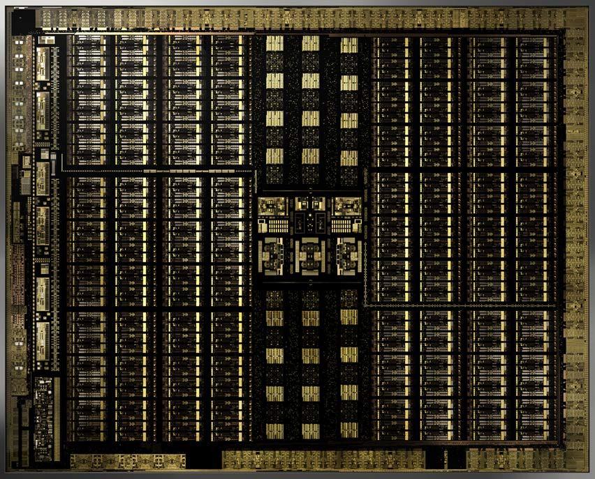
That CPU is really, really impressive.
Wasn't expecting mixed bandwidth for the RAM. I assume OS reserve will come from the slower pool
One thing I didn't understand watching the DF analysis is why it has two separate memory pools at different speeds. Rich only mentioned that it couldn't have been made any other way but I didn't get why.
I think there Richard is referencing that it could not be made another way to fit into the "price" they are angling for while achieving performance.
Which price? IDK!
Did anyone only predict 10 GB for games? Curious what that means for Lockhart now.
It's 13.5 for games.
10 of it is "GPU Optimized"
The other 3.5 is the slower grouping but it all shows as a unified pool. Speed is dictated by which pool the devs hits with the call with the slower groups meant more for things like sound and CPU processes.
It's not 10 GB for games.
16 GB GDDR6
10 GB "Optimal" GPU use (560 gb/s I think) Specifically made to feed the GPU.
3.5 GB "Standard" use (336 gb/s), think for audio, AI, etc.
2.5 GB reserved for the OS.
So, 13.5 GB for games.
Thanks! Very interesting 🧐 no one predicted that 😆 No doubt it's been dialed in considering the thought that has gone into all other aspects.
Yeah. 6GB for the system would make sense given the nature of quick resume means keeping the game stored in RAM so it can be easily and quickly retrieved by the OS.
Edit: Disregard. 13.5GB/2.5GB split. It'll be interesting to see how spreading a game across both pools can affect performance.
PCs essentially do the same thing, so I don't expect any huge differences.
On the XSX, there are inevitably going to be situations where some GPU stuff is handballed to the slower memory pool, which isn't a thing on PC, virtual memory aside (i.e. running a game at settings that force the GPU to rely on system memory for added storage). While 363GBps is still a fair amount of bandwidth, it's also a reduction of almost half (40%), so the extent to which it impacts performance will depend on just how much memory bandwidth is a factor in what's being rendered. You're probably right that it's generally not going to be a big deal, though.
Can Dark1x further explain the reasons for the memory being designed the way it is? Even as a Sr. Systems Engineer this is probably the only aspect that escapes me.
As I previously posted months ago about the mixed memory chip approach and how it will split the RAM bandwidth into two different tiers, apparently this is what MS is going with. Whatever mix of 1GB and 2GB chips MS would have used, every possible setup would have resulted in 10GB of full-speed memory (560GB/s) and a slower pool. In order to have the full 560GB/s for all the memory pool, MS would have had to go with x10 1GB chips (10GB) or x10 2GB chips (20GB). I'm guessing that's what MS's engineers meant was that for a full 560GB/s across the board, they would have needed to have 4 more GB of RAM and that was just too expensive.
So here is the short explanation of why the RAM bandwidth is split into two different speeds. The way GDDR achieves its high speeds is by using parallelism. A single 14Gbps GDDR6 chip (the chips MS is using) can achieve 56GB/s over a 32-bit bus. With two chips, 56GB/s each, using two 32-bit controllers (64-bit) they could achieve 112GB/s and so forth. MS is using 10 chips on a 320-bit bus (32-bit x 10) which will result in 56GB/s x10 -> 560GB/s. So if we will use the classic setup, we got 560GB/s across the board. If a developer needs a texture in RAM, they will split it and spread it around the 10 chips so when it's time to read it, each part will be read at 56GB/s from each chip so the texture will be read from all 10 chips in parallel at 560GB/s. So we've established that the way GDDR6 achieves high speeds is by using parallelism, but what happens when the chips are mixed?
Let's see how GDDR6 would have worked if MS was using the classic setup. This imaginary XSX has x10 2GB chips, a full 20GB setup, each one is able to achieve 56GB/s. It would have looked something like this:
Code:
Chip num  | C01 | C02 | C03 | C04 | C05 | C06 | C07 | C08 | C09 | C10 |
1GB block |     |     |     |     |     |     |     |     |     |     |
1GB block |     |     |     |     |     |     |     |     |     |     |
As you can see, we have 10 chips (C1 through C10) and each one has two blocks, 1GB each (obviously it's simplifying things, chips have millions of blocks). Now let's assume 10GB is already taken and we need to use a huge texture in that memory, a 10GB texture.
Code:
Chip num  | C01 | C02 | C03 | C04 | C05 | C06 | C07 | C08 | C09 | C10 |
1GB block |  X  |  X  |  X  |  X  |  X  |  X  |  X  |  X  |  X  |  X  |
1GB block | T | T | T | T | T | T | T | T | T | T |T = Used by our texture
When the game tries to read that texture, it will read it from all 10 chips at the same time. Each chip will send the relevant block at 56GB/s, so all 10 chips in parallel will provide the system with all the texture data at 560GB/s. Now let's look at how the XSX setup looks like with a mix of 2GB and 1GB chips:
Code:
Chip num  | C01 | C02 | C03 | C04 | C05 | C06 | C07 | C08 | C09 | C10 |
1GB block |     |     |     |     |     |     |     |     |     |     |
1GB block |     |     |     |     |     |     |
As you can see, we have chips 1 through 6 with 2 blocks of 1GB (2GB) while chips 7 through 10 only have 1 block of 1GB (1GB). So what happens now? Using the XSX setup, let's look at the same scenario only this time using a 6GB texture because we only have 6GB left if 10GB is already taken:
Code:
Chip num  | C01 | C02 | C03 | C04 | C05 | C06 | C07 | C08 | C09 | C10 |
1GB block |  X  |  X  |  X  |  X  |  X  |  X  |  X  |  X  |  X  |  X  |
1GB block | T | T | T | T | T | T |T = Used by our texture
Now we have a problem, chips C7 through C10 are all full, they have no more available blocks because not all chips are the same size and every piece of data written to memory wants to spread out on all 10 chips in order to enjoy the full 560GB/s bandwidth. So what happens to our texture? It's stuck on 6 chips, not 10. So 6 chips, 56GB/s each, will result in 336GB/s.
That's where the split comes from. It's still the same memory pool, but at some point, the 1GB chips run out of storage space (addresses) and only the 2GB chips have available storage space so once the first 1GB fills on all 10 chips, data can only be stored on 6 chips. That's why 10GB runs at 560GB/s (the first 1GB of every one of the 10 chips) and 6GB runs at 336GB/s (the remaining 6 chips that have an extra 1GB of space).
So MS's current setup looks like this:
------------------10GB @560GB/s------------------
- the full 10GB is available to developers.
-------------------6GB @336GB/s-------------------
- 3.5GB is available to developers.
- 2.5GB is dedicated to the OS.
So developers will have 13.5GB of GDDR6 available, it's one big pool, not split in any way. But because not all chips have the same size, parallelism goes down on some of the address spaces so as result 10GB out of that 13.5GB will perform @560GB/s while 3.5GB will perform @336GB/s. I can totally see why MS was willing to do that, there is a lot of data that doesn't really need high speeds. For instance on PC games will use a split pool, system RAM and the VRAM on the GPU. So while on the GPU the VRAM is very fast, there is a lot of data that sits in the system RAM and system RAM is sub-100GB/s.
The biggest disappointment is that AA batteries are still around.
It is actually one of the best news. Was afraid they would have built in Batterie.
Always have a pair charged for a quick exchange. No wire needed.
So in early March the DF crew are in Redmond with a hands on session with the Series X.... and in early March DF drop a video about a 4TF next gen console. No way Richard goes to the effort of this without insider intel.
I never actually believed it until now but Lockhart is definitely coming. Game on.
I never actually believed it until now but Lockhart is definitely coming. Game on.
Hey, so here's a question about the XSX dev kits we see in the video:
They're really small compared to the XSX. How is that?
Do we think it's because they're using some expensive cooling, like vapor chamber? Or are they super loud? How can they be so small?
They're really small compared to the XSX. How is that?
Do we think it's because they're using some expensive cooling, like vapor chamber? Or are they super loud? How can they be so small?
I hope on the 18th, they will trailers and gameplay of next-gen games so the detractors of HB2 and Mara graphics will be shut.
Great work! 👍As I previously posted months ago about the mixed memory chip approach and how it will split the RAM bandwidth into two different tiers, apparently this is what MS is going with. Whatever mix of 1GB and 2GB chips MS would have used, every possible setup would have resulted in 10GB of full-speed memory (560GB/s) and a slower pool. In order to have the full 560GB/s for all the memory pool, MS would have had to go with x10 1GB chips (10GB) or x10 2GB chips (20GB). I'm guessing that's what MS's engineers meant was that for a full 560GB/s across the board, they would have needed to have 4 more GB of RAM and that was just too expensive.
So here is the short explanation of why the RAM bandwidth is split into two different speeds. The way GDDR achieves its high speeds is by using parallelism. A single 14Gbps GDDR6 chip (the chips MS is using) can achieve 56GB/s over a 32-bit bus. With two chips, 56GB/s each, using two 32-bit controllers (64-bit) they could achieve 112GB/s and so forth. MS is using 10 chips on a 320-bit bus (32-bit x 10) which will result in 56GB/s x10 -> 560GB/s. So if we will use the classic setup, we got 560GB/s across the board. If a developer needs a texture in RAM, they will split it and spread it around the 10 chips so when it's time to read it, each part will be read at 56GB/s from each chip so the texture will be read from all 10 chips in parallel at 560GB/s. So we've established that the way GDDR6 achieves high speeds is by using parallelism, but what happens when the chips are mixed?
Let's see how GDDR6 would have worked if MS was using the classic setup. This imaginary XSX has x10 2GB chips, a full 20GB setup, each one is able to achieve 56GB/s. It would have looked something like this:
Code:Chip num | C01 | C02 | C03 | C04 | C05 | C06 | C07 | C08 | C09 | C10 | 1GB block | | | | | | | | | | | 1GB block | | | | | | | | | | |
As you can see, we have 10 chips (C1 through C10) and each one has two blocks, 1GB each (obviously it's simplifying things, chips have millions of blocks). Now let's assume 10GB is already taken and we need to use a huge texture in that memory, a 10GB texture.
X = Unavailable blockCode:Chip num | C01 | C02 | C03 | C04 | C05 | C06 | C07 | C08 | C09 | C10 | 1GB block | X | X | X | X | X | X | X | X | X | X | 1GB block | T | T | T | T | T | T | T | T | T | T |
T = Used by our texture
When the game tries to read that texture, it will read it from all 10 chips at the same time. Each chip will send the relevant block at 56GB/s, so all 10 chips in parallel will provide the system with all the texture data at 560GB/s. Now let's look at how the XSX setup looks like with a mix of 2GB and 1GB chips:
Code:Chip num | C01 | C02 | C03 | C04 | C05 | C06 | C07 | C08 | C09 | C10 | 1GB block | | | | | | | | | | | 1GB block | | | | | | |
As you can see, we have chips 1 through 6 with 2 blocks of 1GB (2GB) while chips 7 through 10 only have 1 block of 1GB (1GB). So what happens now? Using the XSX setup, let's look at the same scenario only this time using a 6GB texture because we only have 6GB left if 10GB is already taken:
X = Unavailable blockCode:Chip num | C01 | C02 | C03 | C04 | C05 | C06 | C07 | C08 | C09 | C10 | 1GB block | X | X | X | X | X | X | X | X | X | X | 1GB block | T | T | T | T | T | T |
T = Used by our texture
Now we have a problem, chips C7 through C10 are all full, they have no more available blocks because not all chips are the same size and every piece of data written to memory wants to spread out on all 10 chips in order to enjoy the full 560GB/s bandwidth. So what happens to our texture? It's stuck on 6 chips, not 10. So 6 chips, 56GB/s each, will result in 336GB/s.
That's where the split comes from. It's still the same memory pool, but at some point, the 1GB chips run out of storage space (addresses) and only the 2GB chips have available storage space so once the first 1GB fills on all 10 chips, data can only be stored on 6 chips. That's why 10GB runs at 560GB/s (the first 1GB of every one of the 10 chips) and 6GB runs at 336GB/s (the remaining 6 chips that have an extra 1GB of space).
So MS's current setup looks like this:
------------------10GB @560GB/s------------------
- the full 10GB is available to developers.
-------------------6GB @336GB/s-------------------
- 3.5GB is available to developers.
- 2.5GB is dedicated to the OS.
So developers will have 13.5GB of GDDR6 available, it's one big pool, not split in any way. But because not all chips have the same size, parallelism goes down on some of the address spaces so as result 10GB out of that 13.5GB will perform @560GB/s while 3.5GB will perform @336GB/s. I can totally see why MS was willing to do that, there is a lot of data that doesn't really need high speeds. For instance on PC games will use a split pool, system RAM and the VRAM on the GPU. So while on the GPU the VRAM is very fast, there is a lot of data that sits in the system RAM and system RAM is sub-100GB/s.
AA batteries > Internal
This is coming from a guy who owns the elite 2 controller. If you want a rechargeable battery pack you can buy one.
Include a recharge pack in the box then. Ent got no time for having a bulky AA charger getting in the way.
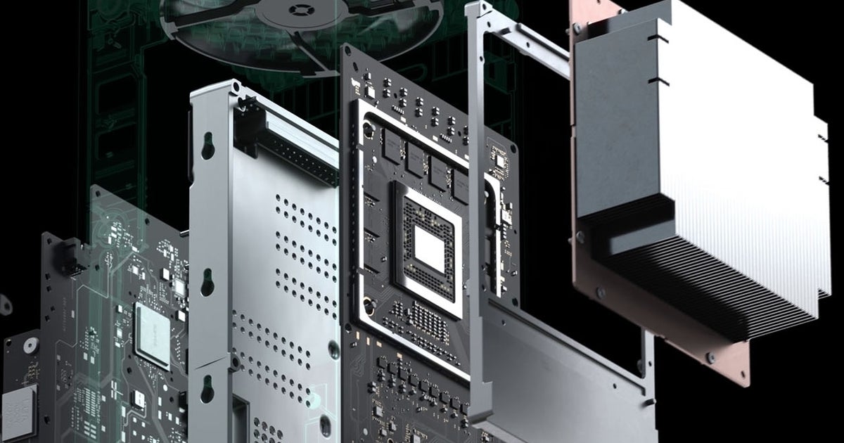
Congrats to Microsoft for a fantastic job on the innards!
pros:
3.6 Ghz CPU baseline is amazing.
The split motherboard design with a single quiet fan is amazing.
GPU @ 1.8 Ghz is amazing.
cons:
The controller was a let down. Where is my adaptive feedback trigger? I want innovation in my controller beyond a better dpad and some grippy texture.
Yeah I wish more innovation was put into the controller. On the other hand MS was able to put all that cost into the main hardware. The manufacturing cost on those controllers have been scaled way down over the years. That's why expecting them to come in at $499.
Valid point.Include a recharge pack in the box then. Ent got no time for having a bulky AA charger getting in the way.
its insane
It's a cost cutting measure, I'm sure. The idea is that 10gb is dedicated to operations that require the most memory bandwidth while the remaining available memory can be used for less critical operations. The OS uses memory from the slower pool.Can Dark1x further explain the reasons for the memory being designed the way it is? Even as a Sr. Systems Engineer this is probably the only aspect that escapes me.
It is a curious thing, though.
I don't think any of us expected that MS would have this in store for us. I recall many guesses of certain specs and those were much lower. I recall plenty comments that certain numbers were too good to be true. Here we are. :)
Good speculation!As I previously posted months ago about the mixed memory chip approach and how it will split the RAM bandwidth into two different tiers, apparently this is what MS is going with. Whatever mix of 1GB and 2GB chips MS would have used, every possible setup would have resulted in 10GB of full-speed memory (560GB/s) and a slower pool. In order to have the full 560GB/s for all the memory pool, MS would have had to go with x10 1GB chips (10GB) or x10 2GB chips (20GB). I'm guessing that's what MS's engineers meant was that for a full 560GB/s across the board, they would have needed to have 4 more GB of RAM and that was just too expensive.
So here is the short explanation of why the RAM bandwidth is split into two different speeds. The way GDDR achieves its high speeds is by using parallelism. A single 14Gbps GDDR6 chip (the chips MS is using) can achieve 56GB/s over a 32-bit bus. With two chips, 56GB/s each, using two 32-bit controllers (64-bit) they could achieve 112GB/s and so forth. MS is using 10 chips on a 320-bit bus (32-bit x 10) which will result in 56GB/s x10 -> 560GB/s. So if we will use the classic setup, we got 560GB/s across the board. If a developer needs a texture in RAM, they will split it and spread it around the 10 chips so when it's time to read it, each part will be read at 56GB/s from each chip so the texture will be read from all 10 chips in parallel at 560GB/s. So we've established that the way GDDR6 achieves high speeds is by using parallelism, but what happens when the chips are mixed?
Let's see how GDDR6 would have worked if MS was using the classic setup. This imaginary XSX has x10 2GB chips, a full 20GB setup, each one is able to achieve 56GB/s. It would have looked something like this:
Code:Chip num | C01 | C02 | C03 | C04 | C05 | C06 | C07 | C08 | C09 | C10 | 1GB block | | | | | | | | | | | 1GB block | | | | | | | | | | |
As you can see, we have 10 chips (C1 through C10) and each one has two blocks, 1GB each (obviously it's simplifying things, chips have millions of blocks). Now let's assume 10GB is already taken and we need to use a huge texture in that memory, a 10GB texture.
X = Unavailable blockCode:Chip num | C01 | C02 | C03 | C04 | C05 | C06 | C07 | C08 | C09 | C10 | 1GB block | X | X | X | X | X | X | X | X | X | X | 1GB block | T | T | T | T | T | T | T | T | T | T |
T = Used by our texture
When the game tries to read that texture, it will read it from all 10 chips at the same time. Each chip will send the relevant block at 56GB/s, so all 10 chips in parallel will provide the system with all the texture data at 560GB/s. Now let's look at how the XSX setup looks like with a mix of 2GB and 1GB chips:
Code:Chip num | C01 | C02 | C03 | C04 | C05 | C06 | C07 | C08 | C09 | C10 | 1GB block | | | | | | | | | | | 1GB block | | | | | | |
As you can see, we have chips 1 through 6 with 2 blocks of 1GB (2GB) while chips 7 through 10 only have 1 block of 1GB (1GB). So what happens now? Using the XSX setup, let's look at the same scenario only this time using a 6GB texture because we only have 6GB left if 10GB is already taken:
X = Unavailable blockCode:Chip num | C01 | C02 | C03 | C04 | C05 | C06 | C07 | C08 | C09 | C10 | 1GB block | X | X | X | X | X | X | X | X | X | X | 1GB block | T | T | T | T | T | T |
T = Used by our texture
Now we have a problem, chips C7 through C10 are all full, they have no more available blocks because not all chips are the same size and every piece of data written to memory wants to spread out on all 10 chips in order to enjoy the full 560GB/s bandwidth. So what happens to our texture? It's stuck on 6 chips, not 10. So 6 chips, 56GB/s each, will result in 336GB/s.
That's where the split comes from. It's still the same memory pool, but at some point, the 1GB chips run out of storage space (addresses) and only the 2GB chips have available storage space so once the first 1GB fills on all 10 chips, data can only be stored on 6 chips. That's why 10GB runs at 560GB/s (the first 1GB of every one of the 10 chips) and 6GB runs at 336GB/s (the remaining 6 chips that have an extra 1GB of space).
So MS's current setup looks like this:
------------------10GB @560GB/s------------------
- the full 10GB is available to developers.
-------------------6GB @336GB/s-------------------
- 3.5GB is available to developers.
- 2.5GB is dedicated to the OS.
So developers will have 13.5GB of GDDR6 available, it's one big pool, not split in any way. But because not all chips have the same size, parallelism goes down on some of the address spaces so as result 10GB out of that 13.5GB will perform @560GB/s while 3.5GB will perform @336GB/s. I can totally see why MS was willing to do that, there is a lot of data that doesn't really need high speeds. For instance on PC games will use a split pool, system RAM and the VRAM on the GPU. So while on the GPU the VRAM is very fast, there is a lot of data that sits in the system RAM and system RAM is sub-100GB/s.
It's not a latency thing is it? I used to read that GDDRx was faster but higher latency than equivalent DDRx, but haven't read that sort of thing in a few years.It's a cost cutting measure, I'm sure. The idea is that 10gb is dedicated to operations that require the most memory bandwidth while the remaining available memory can be used for less critical operations. The OS uses memory from the slower pool.
It is a curious thing, though.
Right. Never. https://www.wired.com/2013/11/playstation4-teardown-video/Can't believe they showed all parts when putting it together, they're extremely transparent here, I've never seen anything like it before. I can imagine Sony is studying this video verrrrry closely.
But alas, something isn't perfect for them yet . Lol 😂 never endingI don't think any of us expected that MS would have this in store for us. I recall many guesses of certain specs and those were much lower. I recall plenty comments that certain numbers were too good to be true. Here we are. :)
Indeed. Anyway, i think we can all agree Series X would be a fantastic value if they hit $499 comparing to gaming PCs. Interesting times ahead!It's a cost cutting measure, I'm sure. The idea is that 10gb is dedicated to operations that require the most memory bandwidth while the remaining available memory can be used for less critical operations. The OS uses memory from the slower pool.
It is a curious thing, though.
Yes, it's a better setup than 56 @1.7Ghz. For instance, 1.675Ghz will be 107.2GP/s fillrate while a 1.825Ghz will be 116.8GP/s (assuming 64 ROPs like the Github leak). So as you can see, higher frequency effects other areas of the GPU, even though everyone likes focusing on the TF count.It was believed the GPU would have 56 CU active at ~1.675 GHz but with 52 CU at 1.85 GHz, the rest of the GPU also benefits, right?
I made a post about that a while ago:My knowledge does run run that deep anymore, but I know enough that all these specs impress me and surpass some of my expectations. My only (slight!) letdown in the amount of RAM?
Someone who is smarter than me: Thoughts on the RAM situation? I assume now that the XSX is equipped with an NVME SSD it'll use that as a sudo-RAM (Virual RAM) albeit slower, once it allocated all 16GBs? GDDR6 is fairly speedy, correct?
Thanks!!

PS5 and Xbox Series speculation |OT11| Cry Havoc and Let Slip the Dogs of War [NEW NEWS, NEW THREAD - CHECK OUT THE STAFF POST]
unless they are doing a universal launch. Jim Ryan of Sony has already hinted that they are. Plus, PlayStation Japan tweeted about a holiday 2020 launch. If that’s the case, they’ll have to start manufacturing well before June.
 www.resetera.com
Thanks, but it's not speculation considering that's how GDDR works. If they mix the chips, they will have two different speeds :)
No way they'd let it go that easy.be in a quality/performance toggle?
and I told yall pathtraced Minecraft was gonna be for consoles. though I'm surprised they only had one person on it so far
It's a cost cutting measure, I'm sure. The idea is that 10gb is dedicated to operations that require the most memory bandwidth while the remaining available memory can be used for less critical operations. The OS uses memory from the slower pool.
It is a curious thing, though.
I'm confused on a quote that was shared on the Digital Foundry article. There is a quote that says "Our second component is a high-speed hardware decompression block that can deliver over 6GB/s," reveals Andrew Goossen.", but on the same article the specs table has the transfer rate at 2.4GB/s (Raw) or 4.8GB/s (Compressed). Was this a typo or I'm reading something wrong? Dictator
Inside Xbox Series X: the full specs
This is it. After months of teaser trailers, blog posts and even the occasional leak, we can finally reveal firm, hard …
Last edited:
The speculation bit was about how the memory would be allocated. We knew (or suspected) the amount and BW from the game awards reveal. That was good insight.Yes, it's a better setup than 56 @1.7Ghz. For instance, 1.675Ghz will be 107.2GP/s fillrate while a 1.825Ghz will be 116.8GP/s (assuming 64 ROPs like the Github leak). So as you can see, higher frequency effects other areas of the GPU, even though everyone likes focusing on the TF count.
I made a post about that a while ago:
PS5 and Xbox Series speculation |OT11| Cry Havoc and Let Slip the Dogs of War [NEW NEWS, NEW THREAD - CHECK OUT THE STAFF POST]
unless they are doing a universal launch. Jim Ryan of Sony has already hinted that they are. Plus, PlayStation Japan tweeted about a holiday 2020 launch. If that’s the case, they’ll have to start manufacturing well before June.
Thanks, but it's not speculation considering that's how GDDR works. If they mix the chips, they will have two different speeds :)
impressive specs...PC will still be better because the upgrade cycle is faster...with the new generation of Nvidia/AMD GPU's coming later this year it should put some distance between the new consoles
what are the rumors about the PS5 specs?...has Sony conceded that they will lose in terms of raw computing power?...as long as they are somewhat close Sony will be fine, their PS exclusives will more then make up for it
what are the rumors about the PS5 specs?...has Sony conceded that they will lose in terms of raw computing power?...as long as they are somewhat close Sony will be fine, their PS exclusives will more then make up for it
[/QUOTE]
MS is saying holiday 2020. they arent guessing.
MS is saying holiday 2020. they arent guessing.
no, that's literally how you calculate it, and uh, amd has been doing raytracing just as long as nvidia has. as for R&D..... amd makes a habit of spending nearly no cash and still bringing giants to their knees, they did it to intel, they can do it to nvidia. Nvidia's implimentation on turing is completely ridiculous, and performance is crap because of a few decisions they made with it, but then amd patented all the faster ways they could have done it, so there's that. rdna2 just has 4x as many RT cores at any given shader count than nvidia, so they're ~4x faster on paper. In practice its more than that, for example, on turing, doing any kind of RT op on any given SM basically locks out any other use of the SM until its done, and the RT core has to wait until it has 32 completed rays, or they're about to do a context switch, to yeet that data back to the shaders so they can continue working. AMD has no such limitation, the shaders can happily do other, unrelated things while the RT cores are working I'd be happy to dive into details on it but its rather dull and most here wont care or won't believe me anyway.
I don't believe this is the case. I'm not that deep into graphics, but isn't Turing also using a hybrid approach to Raytracing, similar to AMD? RT cores and SMs are working independenly from each other, which makes sense considering a lot of the shading is still done in the CUDA cores.
NVIDIA Turing Architecture In-Depth | NVIDIA Technical Blog
Fueled by the ongoing growth of the gaming market and its insatiable demand for better 3D graphics, NVIDIA® has evolved the GPU into the world’s leading parallel processing engine for many…
 devblogs.nvidia.com
Both Ray tracing and Rasterization pipeline operate simultaneously and cooperatively in Hybrid Rendering model used in Turing GPUs.
As someone in the habit of leaving a lot of games installed, I like having the option to expand with a second NVMe drive (even if it is proprietary, likely expensive). I imagine that you can still download and copy games to an external USB drive, though some may have to be moved to an NVMe to play (or at least for optimal performance).
They may be confident it launches holiday 2020 but they aren't certain. Nobody's certain of anything that far out yet.
Always listen to Mat when it comes to these things.
Brad Sams had mentioned it
Doubt it. 10GB of it is dedicated to the GPU plus streaming from the SSD. The $1200 2080 ti is 11GB for perspective.
wow
Woah. I've never seen that.
WTF would you need 24 gigs of ram for?
Even 4K textures dont take up 16 gigs so why 24?
GPU side you need RAM for new rendering techniques, raytracing acceleration structures, textures, etc. CPU side there's obviously the whole game logic/world state tied to it. Some of that can be offloaded to the SSD, but the percentage in real application will not be as high as some do hope for.
Regarding memory for textures: Its not a fixed cost. The more memory you have, the more you can spend on textures.
"4K" in conjunction with textures is mostly a marketing term, as each texture has a different resolution that is completely independent from rendering resolution. Some textures don't need to be 4K, while for others 4K is not enough. It all depends on the size of the object/surface the texture is mapped to and the minimal distance the camera can approach to said object. Also, the texture information for each pixel of rendered surface is not the result of a single texture but multiple ones that are combined with each other.
The biggest disappointment is that AA batteries are still around.
Switch pro controller shows you don't need AA batteries for good battery life!
I much prefer having batteries. I always have an extra set of Eneloops ready to go. When my PS4 controller battery dies (which is OFTEN) I have to play tethered if I want to keep playing. Hate it.
my #1 issue is will I have enough room for it to shed heat properly
my xbox cubby is 11" tall by 17" wide
If I want this thing in there I wonder if 2.5" of space on either side horizontally is enough to allow proper cooling or if it will just blow the hot air back at itself
my xbox cubby is 11" tall by 17" wide
If I want this thing in there I wonder if 2.5" of space on either side horizontally is enough to allow proper cooling or if it will just blow the hot air back at itself
As I previously posted months ago about the mixed memory chip approach and how it will split the RAM bandwidth into two different tiers, apparently this is what MS is going with. Whatever mix of 1GB and 2GB chips MS would have used, every possible setup would have resulted in 10GB of full-speed memory (560GB/s) and a slower pool. In order to have the full 560GB/s for all the memory pool, MS would have had to go with x10 1GB chips (10GB) or x10 2GB chips (20GB). I'm guessing that's what MS's engineers meant was that for a full 560GB/s across the board, they would have needed to have 4 more GB of RAM and that was just too expensive.
So here is the short explanation of why the RAM bandwidth is split into two different speeds. The way GDDR achieves its high speeds is by using parallelism. A single 14Gbps GDDR6 chip (the chips MS is using) can achieve 56GB/s over a 32-bit bus. With two chips, 56GB/s each, using two 32-bit controllers (64-bit) they could achieve 112GB/s and so forth. MS is using 10 chips on a 320-bit bus (32-bit x 10) which will result in 56GB/s x10 -> 560GB/s. So if we will use the classic setup, we got 560GB/s across the board. If a developer needs a texture in RAM, they will split it and spread it around the 10 chips so when it's time to read it, each part will be read at 56GB/s from each chip so the texture will be read from all 10 chips in parallel at 560GB/s. So we've established that the way GDDR6 achieves high speeds is by using parallelism, but what happens when the chips are mixed?
Let's see how GDDR6 would have worked if MS was using the classic setup. This imaginary XSX has x10 2GB chips, a full 20GB setup, each one is able to achieve 56GB/s. It would have looked something like this:
Code:Chip num | C01 | C02 | C03 | C04 | C05 | C06 | C07 | C08 | C09 | C10 | 1GB block | | | | | | | | | | | 1GB block | | | | | | | | | | |
As you can see, we have 10 chips (C1 through C10) and each one has two blocks, 1GB each (obviously it's simplifying things, chips have millions of blocks). Now let's assume 10GB is already taken and we need to use a huge texture in that memory, a 10GB texture.
X = Unavailable blockCode:Chip num | C01 | C02 | C03 | C04 | C05 | C06 | C07 | C08 | C09 | C10 | 1GB block | X | X | X | X | X | X | X | X | X | X | 1GB block | T | T | T | T | T | T | T | T | T | T |
T = Used by our texture
When the game tries to read that texture, it will read it from all 10 chips at the same time. Each chip will send the relevant block at 56GB/s, so all 10 chips in parallel will provide the system with all the texture data at 560GB/s. Now let's look at how the XSX setup looks like with a mix of 2GB and 1GB chips:
Code:Chip num | C01 | C02 | C03 | C04 | C05 | C06 | C07 | C08 | C09 | C10 | 1GB block | | | | | | | | | | | 1GB block | | | | | | |
As you can see, we have chips 1 through 6 with 2 blocks of 1GB (2GB) while chips 7 through 10 only have 1 block of 1GB (1GB). So what happens now? Using the XSX setup, let's look at the same scenario only this time using a 6GB texture because we only have 6GB left if 10GB is already taken:
X = Unavailable blockCode:Chip num | C01 | C02 | C03 | C04 | C05 | C06 | C07 | C08 | C09 | C10 | 1GB block | X | X | X | X | X | X | X | X | X | X | 1GB block | T | T | T | T | T | T |
T = Used by our texture
Now we have a problem, chips C7 through C10 are all full, they have no more available blocks because not all chips are the same size and every piece of data written to memory wants to spread out on all 10 chips in order to enjoy the full 560GB/s bandwidth. So what happens to our texture? It's stuck on 6 chips, not 10. So 6 chips, 56GB/s each, will result in 336GB/s.
That's where the split comes from. It's still the same memory pool, but at some point, the 1GB chips run out of storage space (addresses) and only the 2GB chips have available storage space so once the first 1GB fills on all 10 chips, data can only be stored on 6 chips. That's why 10GB runs at 560GB/s (the first 1GB of every one of the 10 chips) and 6GB runs at 336GB/s (the remaining 6 chips that have an extra 1GB of space).
So MS's current setup looks like this:
------------------10GB @560GB/s------------------
- the full 10GB is available to developers.
-------------------6GB @336GB/s-------------------
- 3.5GB is available to developers.
- 2.5GB is dedicated to the OS.
So developers will have 13.5GB of GDDR6 available, it's one big pool, not split in any way. But because not all chips have the same size, parallelism goes down on some of the address spaces so as result 10GB out of that 13.5GB will perform @560GB/s while 3.5GB will perform @336GB/s. I can totally see why MS was willing to do that, there is a lot of data that doesn't really need high speeds. For instance on PC games will use a split pool, system RAM and the VRAM on the GPU. So while on the GPU the VRAM is very fast, there is a lot of data that sits in the system RAM and system RAM is sub-100GB/s.
nice!
It has connector interconnect. Like first revisions of PS2.
I'll take MS's continued assurance its holiday 2020 over someones speculation
They're still saying holiday 2020 because that's the date they announced months ago.
This is not "continued assurance." They have no way of knowing because they don't know how long this is going to go on for, just like you and I don't know.
But they're also not going to say it no longer has a release date. That is bad and confusing marketing.