I finally did a first sweep of temperature tests on mine.
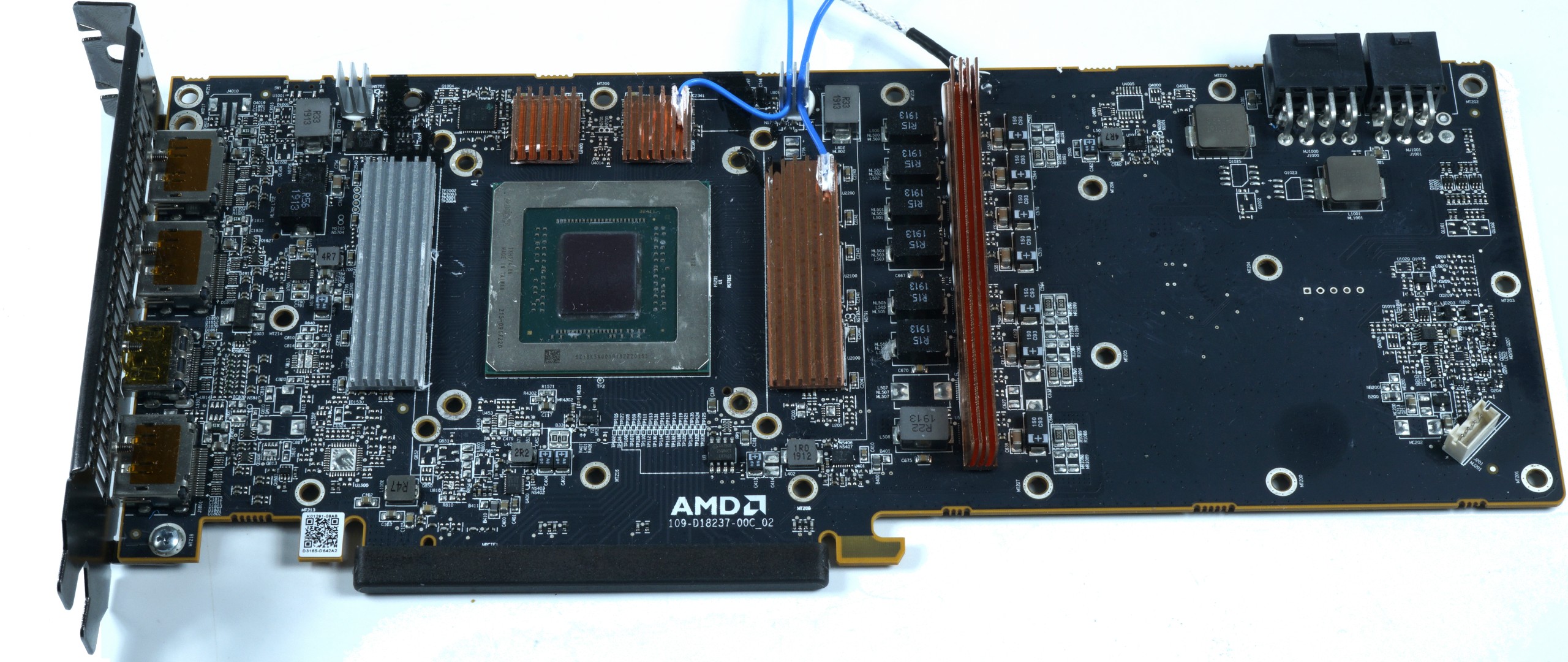
I place a probe carefully in the the center of each ram chip but on the other side of the TIM, so the heat goes through the TIM, and through the thin aluminum layer. Rebuilt the PS5 completely and tested right into my equipement rack, squeezed on the shelf so everything is a real world situation. This won't provide any figures about the efficiency of the TIM, nor the exact die temperature, but it will show if there's an outlier chip that gets hotter, and hint at the possibility of experimental errors from other people's tests if they have outlier values when measuring from the other side of the board.
Code:
[FRONT]
   8  1
7        2      [FAN]
6        3
   5  4
[REAR]

Chip   Youtube(4K)    Astrobot(Memory Level)

1    45.0C        50.5C
2    39.7C        48.8C
3    41.1C        52.6C
4    43.0C        54.4C
5    44.2C        55.2C
6    42.1C        56.6C
7    41.7C        55.6C
8    40.9C        55.0C
The assumption required here is that all TIM on each chip, and the die-to-case characteristics should be almost identical, and each chip should have the same dissipated power. The variation expected would be from airflow, the shape of the aluminum sheet, differences on the PCB and proximity to heat sources.
The thermal resistance comprised of the aluminum thickness is negligible, and while the TIM is unknown, anything correctly applied would be maybe 2C/W on a pad of this area and thickness. The limits we're looking for here is the 95C on the surface of the case, it's up to the chip manufacturer to guarantee those specs, including the GDDR6 packaging for automotive use that allows a 105C case surface temperature (which indicates automotive GDDR6 used in self driving cars would need to be tested to be reliable up to a 120C die, unless they significantly underclock).
Youtube test was just to see what happens with medium-low power consumption, just a 4K playback for about 30 mins. For the Astrobot test I entered the memory level and left the character there for 1 hour (seemed to reach a steady state after about 30 mins). It's not the worst consumption across the entire game, but it allows to redo the exact same test with the sensor placed elsewhere (had to do 3 separate tests, since I only have 3 probes, and I didn't want to fill the precious space over the aluminum sheet with 8 wires that would really mess up the airflow). I'll be able to redo an exact test after the TIM is tore off or replaced. and I might test again after drilling a tiny hole in the aluminum plate to put a sensor right on the surface of the chip.
So there isn't any outlier chip. It shows 1 2 3 are being cooled a little better by their proximity to the aluminum area closest to the fan, and 4 5 6 7 8 being on the other side and under the optical drive so that surface area of the aluminum heatsink isn't getting as much cooling. All of the chips are an equal distance from the main heat source too. The chip closest to the NAND controller could have been an issue, but it doesn't seem to show anything.
A 20C higher die than the point of measurement here would be reasonable, the math adds up to 15C junction to case, 5C through the TIM, and negligible through the aluminum thickness. However the GDDR6 specs is 95C case surface temperature, leading to a calculated limit of 110C junction, as opposed to GDDR5 which was 85C case limit, and 100C junction.
Other people's tests on GDDR6 confirm the 15C delta we should expect from GDDR6 between the die and the case surface:
All the errors and confusions about the suddenly occurring value of the memory temperatures of AMD’s current graphics cards understandably lead to uncertainty among many users. Modern memory chips…

www.igorslab.de
Basically my test is closer to the case temperature (JEDEC requirements), while GN and Spawn Wave tests are measuring almost directly the die temperature (a much more important figure for overclockers). And combining all of this with 15C junction-to-case, and 5C through the TIM, it's all adding up except for the GN outlier chip. Spawn wave is 5C higher than my hottest chip, but I didn't try to find the highest consumption across astrobot so it seems a reasonable difference.
TL;DR
Unless I missed something, the math don't logically add up to more than 70C to 75C chip surface temp (from a 95C allowed design limit) unless there's been ridiculous amount of damage to the TIM, or my Astrobot test is very far from the highest consumption.
Whichever way we try to deduce the actual case surface temperature, to see how close it is from the of the JEDEC requirements, either from the top going through the TIM, or from the bottom, going through the vias, die, and package, I don't see any indication the 95C limit is reached within that thermal sandwich.