The extra GB in the 2GB chips that form the "slow pool" have a different set of memory addresses, so you can intentionally separate contents from the "fast pool" even though they exist together on the same physical chip. But the traces which connect that chip to the SOC aren't doubled. So my understanding is that when you're sending data to the "slow pool", that will negatively impact the speed of the "fast pool". Only 4 chips will be running at full speed, the others will be at a lower percentage depending on how the data for the two address sets is queued/interleaved.
PS5 will also have CPU/GPU contention issues that will reduce its effective RAM bandwidth, though of a different kind.
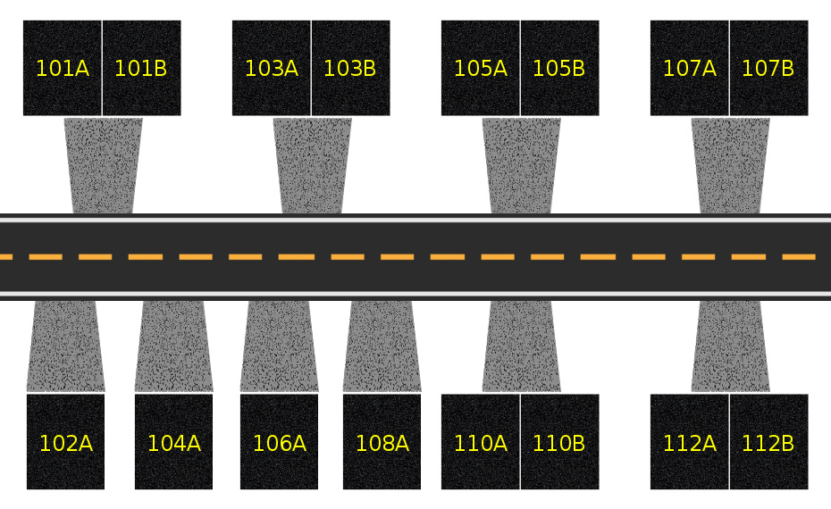
I'm pretty sure most of this is incorrect or mixed up. There are 10 RAM chips, yes. But there's not 4 at 2GB and 6 at 1GB, that would only be 14 GB total. You have the quantity per capacity reversed. Which also means you have the layout wrong--at least one chip on each of the sides is also 2GB. (I don't believe we know whether the layout is 1-4-1 or 2-2-2.)
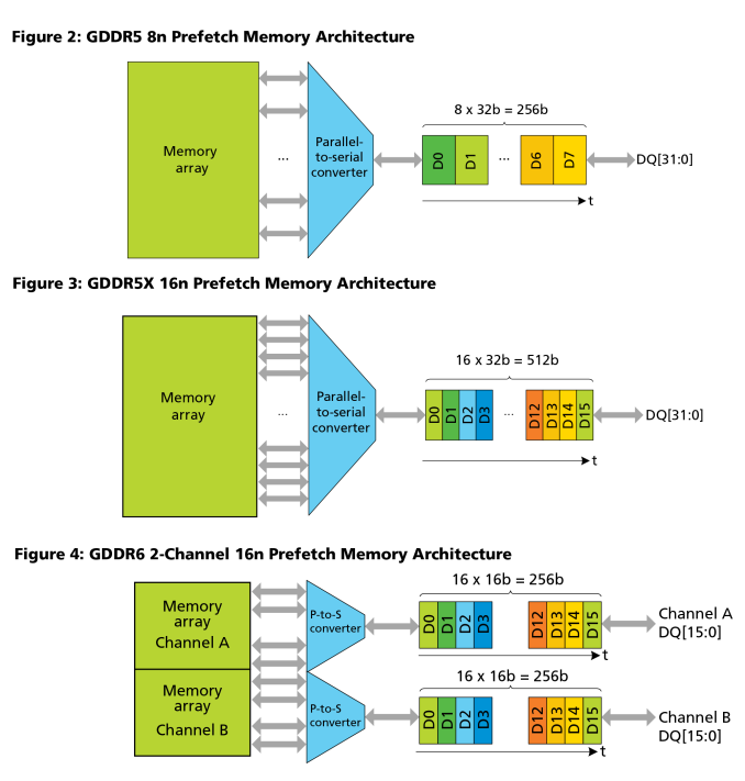
But the more confusing thing is your explanation of speeds and how to derive bandwidth. First, how is "1750MHz" a data rate? Megahertz as units indicates a memory clock speed. But second, no GDDR6 is clocked that high. (We'll see where you actually got the number from below.) Third, why do you call it a
quad data rate (QDR)? GDDR6 uses a double data rate--it's got "DDR" right there in the acronym. Fourth, when you reuse the 1750 figure in your bullet points, the units are now listed as "MT/s", which is proper. But that's not a data rate nor a clockspeed, it's total transfers (T). It's actual clockspeed (875MHz) times transfers per clock (2, for double data rate memory). Fifth, you say to multiply by "the total capacity per chip", but this isn't so for all chips. On the 2GB chips, you can only multiply by the half of the capacity that has the same address range as the others.
Even ignoring your errors, the formula you use can be greatly simplified and made clearer to readers. Instead of the elaborate string of factors, some of which have units people aren't generally familiar with, I think it makes more sense to put it this way:
Bus size (bits) = [number of chips] x 32
Bandwidth (GB/s) = [bus size (bits)] x [chip data rate (gbps)] / 8 (bits per byte)
For PS5, there are 8 2GB chips at 14gbps. So {8 x 32} means the bus is 256-bit. {256 x 14 / 8} means the bandwidth is 448 GB/s.
XSX is a touch more complicated because there are 10 physical chips at 14gbps, but 6 of them are 2GB and 4 are 1GB. Think of the chips as homes along a street, with 4 single homes with driveways and 6 duplexes of double size which share a driveway. There are 10 addresses that end in A, and 6 addresses that end in B.
Each home represents a gigabyte of capacity, but the A and B addresses in the duplexes can't use the shared driveway at the same time. So we can consider the A addresses alone, where the bus size is {10 x 32} or 320-bit. {320 x 14 / 8} means the bandwidth is 560 GB/s. Or we can consider the B addresses alone, where the bus size is {6 x 32} or 192-bit. {192 x 14 / 8} means the bandwidth is 336 GB/s. Note that when the 6GB of B addresses are being filled or emptied, you can only fill or empty 4GB of "GPU-optimal" A addresses, at a bandwidth of {4 x 32 x 14 / 8} or 224 GB/s. When the 10GB of A addresses are being filled or emptied, you can't fill or empty the CPU/OS 6GB at all.
Of course, neither of those extremes will be reached. The two address sets will instead alternate using the interfaces ("driveways") very rapidly. But this does mean that due to these conflicts, the average bandwidth won't reach the 560 GB/s ceiling. (This is true for all unified memory pools, including PS5.)
The map thing is talking about what kinds of situations cause power use to go up. It's obvious that one way is to go from very simple game engines to much more complicated and powerful ones. A simple indie game doesn't require as many calculations as quickly as a AAA showpiece,, so less wattage is used. But the point Mr. Cerny was making was about a counterintuitive fact that at some point, making the workflow more complicated actually requires less power.
This is because if a developer devises long and elaborate calculations, each step may need multiple input values, which themselves have to be calculated. If even one of the input steps takes longer than the rest, the overall calculation stalls because the following step can't start. At a certain point, too many stalls means framerate or IQ suffers as the GPU is no longer able to go fast enough to finish each frame in time. Developers optimize to reduce stalls and avoid this, but they also try to improve results, meaning stalls are never wholly eliminated. So in very advanced games, the GPU is not truly saturated, because some of it is waiting around for work.
Take a highly-optimized engine and give it something straightforward to do, though, and it can shove simple instructions through the GPU as fast as the silicon can go, with no stalls. So
Horizon's menu screen suddenly is using every single transistor all the time, and power use spikes.
The intent of controlling CPU/GPU frequency by monitoring activity rather than temp is to be able to immediately detect these "supermax" usage events, and reduce the clock accordingly. That has no effect on rendering, because the associated workloads are simple and can be completed at pace even with lower clockspeed. But it allow you to eliminate all the highest power spikes a constant-frequency chip would face. So you can now design a cooling solution just good enough for the lower maxima=um hit by advanced gameplay scenarios and their semi-stalled activity. That saves size, cost, and noise.