Cheers. I certainly have no regrets so far.
I know that cu size is just one factor that contributes to overall APU size, but if 20 Navi compute units takes up so little relative die space then what're the chances that the final chip will have only 36 cu (i.e. github leak)
It's not just the extra CUs you need to consider. You also need additional memory bandwidth to feed them. So 20 additional CUs might bump you up to a bigger bus width, impacting the silicon footprint for PHYs and i/o logic on the die.
I start to believe the PS5 devkit-design could be the final design of the PS5 or looks similar at least.
Let's check the devkits of PS1, PS3 and PS5 first. You could also look at the devkits of the original XBOX, GameCube and Dreamcast as a bonus. Remarkably, all these more looks like a tower PC / rack workstation than a console. And as we all know they have nothing to do with the final product.
Next let's check the PS2 DevKit:
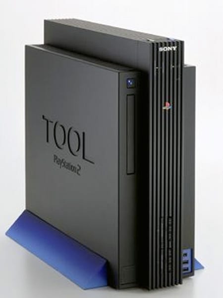
It's very striking the DevKit looks similar to the final product. Expressed in a simple way you only need to remove the left box/extension to nearly get the final PS2 design.
After I saw that I noticed the following facts:
1. The PS2 devkit is the only PlayStation DevKit which looks like the final console (it's only significantly larger and has this Extension on the lft)
2. It Looks completely different compared to the other DevKits from Sony and some of their competitor
Next I researched the official design-registrations from PS2, PS3, and PS4 consoles and devkits:
PS2 (Release: 04-03-2000)
Console: Application date 10-12-1999, priority date 26-08-1999 (design number: 99077509)
DevKit: Application date 10-12-1999, priority date 26-08-1999 (design number: 99077507)
PS3 (Release: 11-11-2006)
Console: Application date 21-10-2005, priority date 16-05-2005 (design number: 000419411-0001)
DevKit: Application date 18-10-2006, priority date 08-05-2006 (design number: 000610860)
PS4 (Release: 15-11-2013)
Console: Application date 12-11-2013, priority date 16-05-2013 (design number: 302013005786)
DevKit: Application date 31-05-2016, priority date 02-12-2015 (design number: 302016002257)
PS5
DevKit: Application date 28-05-2019, priority date 30-11-2018 (design number: 302019002287)
You can also check the registrations @ https://www.tmdn.org/tmdsview-web/welcome.html#. Use the advanced search and copy&paste the design numbers at the design number field.
When checking the list there is one interesting fact: While the PS3 and PS4 devkit designs where registiered noticeably after the console-design itself (and the PS4 devkit after the official release), the design of the PS2 devkit and the console itself where registered at the exact same date - also the priority date is exaclty the same.
So, summarized after seeing all of these facts I came to the solution it could be quite possible the PS5 devkit shows the final console design in any way. Furthermore the devkits of the PS2, PS3 and PS4 where monsters compared with the final products. After we still saw some PS4 Controllers near to the PS5 devkit the devkit is definitely smaller than any of the previous ones.
Logically it could just be Sony goes another way for the actual console generation, registiered the devkit earlier and the final console will have a complete other design - or I did a mistake on my search.
Nice post.
Not having to download to play a game. Or download while streaming. Simple things. Streaming isn't just not having a console.
None of the things you mention require any deeper platform level integration. PS Now does all that already.
Streaming in next-gen consoles is essentially a thin client app. I don't think there's anything more revolutionary on the streaming side that will be effected by streaming on next-gen hardware.
The big benefits of streaming as I said are not needing local hardware at all, plus the possibility of leveraging greater-than-local-hardware performance per user.
More CUs = More heat + lower yields + more silicon used per chip + more wasted silicon on the wafer = more expensive.
You have a BOM goal and the vision of the console and you do the best you can with that in mind.
Incidentally, everyone forgets that faster clocks also reduces manufacturing yields.
Outside of dies rejected on the basis of silicon defects, not every die coming off the line will meet the target clockspeed at or below the requisite target voltage threshold.
It's the biggest reason why I don't believe a 36CU @ 2GHz console APU is realistic.
We really don't know what is possible. The 5500 uses a single SE for 24 CUs (22 enabled), so who knows what is possible. If the 5800 is ~60 CU (just a guess because the 56 CUs that are probably in the XSX), then it might have the exact same 2 SEs as the 5700, it might have bigger SEs but still just 2, it might have 3 similar SEs and it can also have 4 smaller SEs. We just don't know and I think it will take a few months until we do. We might even see the XSX or PS5 or both before we see the 5800 or 5900 considering GPUs are usually announced just weeks before release.
I dunno. From the RDNA whitepaper it sounds pretty cut and dry. The functional blocks in the SE front end can have their quantities scaled for larger WGP counts per SA or larger SAs per SE.
It's why i'm expecting big Navi to still remain with 2x SEs, but just increase the SA count per SE and scale the number of geometry processors, ACEs, beef up the command processor etc in the SE front end.