We are going to be okay anyway, the question is if the platform holder are :)
For sure. Battle for my coins!
We are going to be okay anyway, the question is if the platform holder are :)
Cost per wafer. Size of chip. Yields. All of this is important when considering price. Have you seen how big NVIDIAs big GPUs are? The 2080 is 545mm2 on 12nm. The 5700xt by comparison is 251mm2 on 7nm.
Scorpio APU is 359mm2 on 16nm. We estimate the Series X APU to be around 380mm2. Very similar. Wafers are more expensive at 7nm but yields are good so the price won't much different. Consoles get orders in the millions. We're going to be ok.
I'm not worried at all, personally my expectations for the PS5 is somewhere between a 5700 and 5700XT with a bunch of added features bolted on.
With that in mind I can see between mid 8Tflops and low 9Tflops for PS5.
I still think the XSX is sub 10 RDNA Tflops but we will see for sure soon.
I'll take my stab at it. I envision a chiplet configuration with a small bank of HBM directly on the interposer.
The specific configuration can be found here:


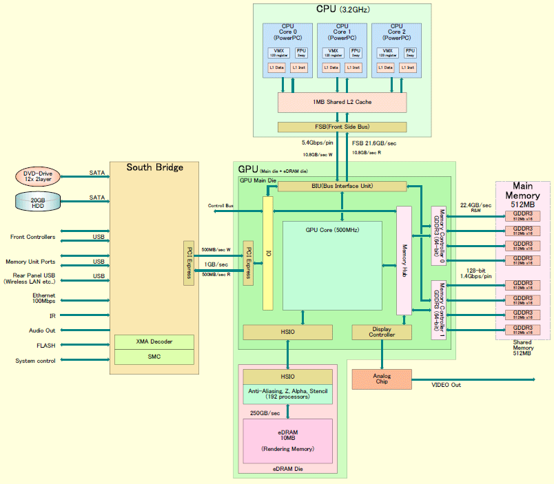
Indeed they did crazy stuff. Wasn't it several steps until it was one chip. First 2 chips, then MCM and then single chip? I do not remember.Having memory stacked on top of the GPU die is definielty future stuff.
But just having a simple MCM APU with a CPU-Chiplet connected to the GPU which has the Memory-Controllers and then talking to GDDR6 would be relatively easy to do.
The Xbox 360 followed that concept and with newer process nodes they put the CPU and GPU on the same chip later on.
They did "crazy" stuff back then.
Precisely. And low margin GPUs make up a majority of the sales. A lot more people buy 1650, 1660, and 2060s than they do 2080 and 2080 TIs.This is not linear, the gross margin of lower end GPU is probably lower than 64% and the gross margin of Turing GPU is probably higher. On the table I gave the lowest Nvidia GPU is only price 50% above manufacturing cost the highest Nvidia GPU price is 143% above the manufacturing cost.
Don't be concerned about resolution gate, it will be replaced by NVMe based milliseconds of loading screens :)As long as both console is on parity i am good otherwise it will be resolution gate all over again lol
There are going to be seconds of difference. I'd bet on a ~2x difference of loading speed.Don't be concerned about resolution gate, it will be replaced by NVMe based milliseconds of loading screens :)
This is not linear, the gross margin of lower end GPU is probably lower than 64% and the gross margin of Turing GPU is probably higher. On the table I gave the lowest Nvidia GPU is only price 50% above manufacturing cost the highest Nvidia GPU price is 143% above the manufacturing cost.
First it were two chip packages.Indeed they did crazy stuff. Wasn't it several steps until it was one chip. First 2 chips, then MCM and then single chip? I do not remember.
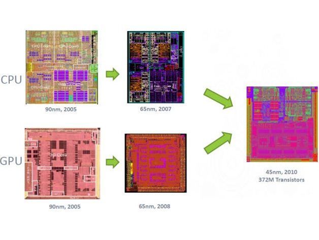

Well, we estimated the die size of the X to be 380-400nm. If the 5700xt is 250mm2 and the zen 2 CPU is around 50mm2 (maybe smaller depending on the cuts to cache) so we still have 80mm2 -100mm2 to work with. Memory controller isn't that big so I'm going to assume many more CUs.
As long as both console is on parity i am good otherwise it will be resolution gate all over again lol
Ok so I'm going to put forth and clarify my thinking:
the XSX is the equivalent of 12 GCN Tflops or 2x X1X
XSX is actually 9.6 RDNA Tflops
PS5 is actually 9.2 RDNA Tflops
This makes:
Phil's statements true
rumors that both are close true
That XSX slightly out performs PS5 true
9 Tflop PS5 leaks true
further we already have prospective AMD GPUs which would fall into the needed performance/price range for this to be true
ok I'm adding to this theory and likely going to catch a lot of hate for this, but...maybe the Xbox series X actually uses a chiplet design.
You know there is a photo of the Xbox Series X chip in the public already?ok I'm adding to this theory and likely going to catch a lot of hate for this, but...maybe the Xbox series X actually uses a chiplet design.
-snip-
Nope.ok I'm adding to this theory and likely going to catch a lot of hate for this, but...maybe the Xbox series X actually uses a chiplet design.
You know there is a photo of the Xbox Series X chip in the public already?
(no hate 🤓)
Nope.
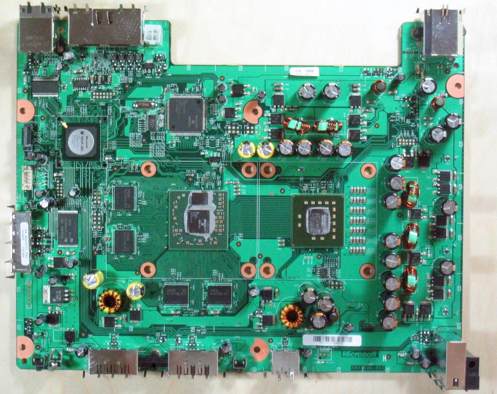
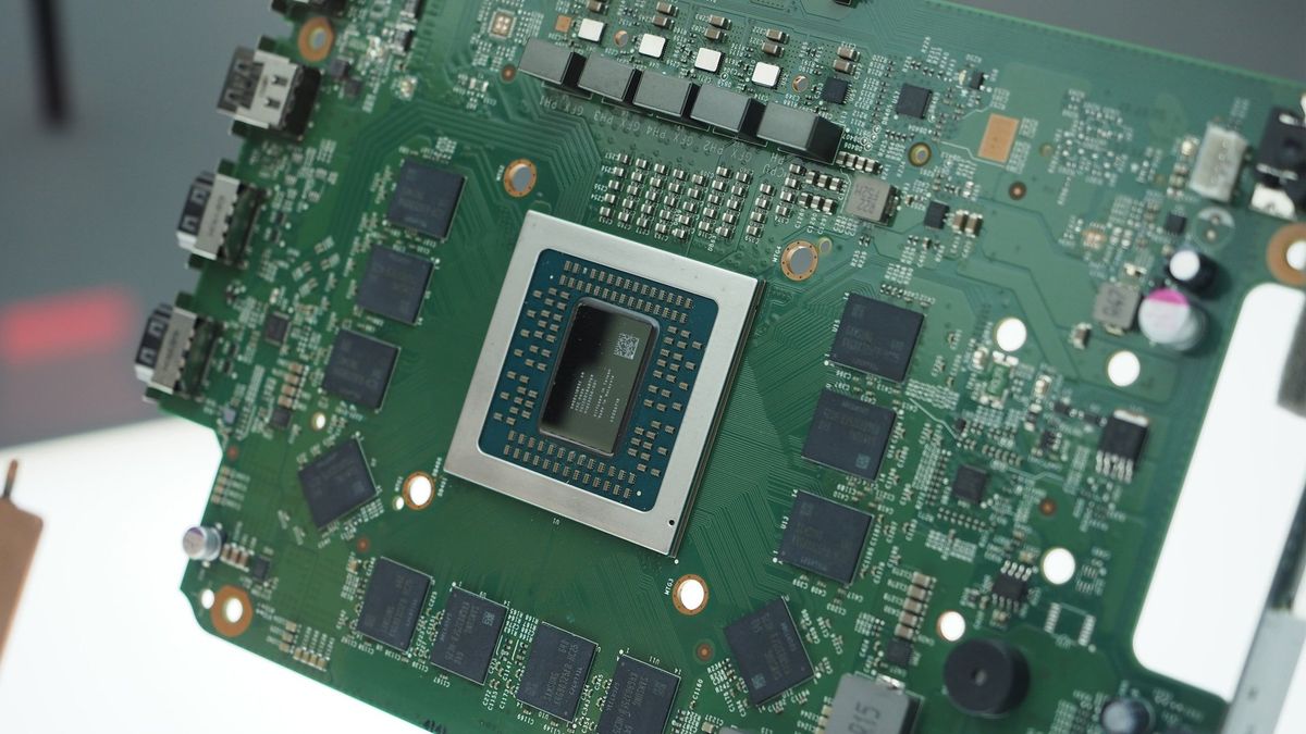
We've already seen the die and it's monolithic.
And I doubt they're clocking their 52 CUs at 1450 MHz. That would make the X1X a bigger jump in clock to the S than the SX is to the 1X.
I told you this yesterday.
This is the way /mandoWhat's up with 2-3 week old accounts causing a ruckus every few days?
Ok so I'm going to put forth and clarify my thinking:
the XSX is the equivalent of 12 GCN Tflops or 2x X1X
XSX is actually 9.6 RDNA Tflops
PS5 is actually 9.2 RDNA Tflops
This makes:
Phil's statements true
rumors that both are close true
That XSX slightly out performs PS5 true
9 Tflop PS5 leaks true
further we already have prospective AMD GPUs which would fall into the needed performance/price range for this to be true
Tom Warren teased 12TF since X019, and this WC article posted before TGAs reveal:This seems all plausible to me. Where did the 12 teraflop report come from btw?
 www.windowscentral.com
Series X won't be 9.6TF and Ps5 won't be 9.2TFThis seems all plausible to me. Where did the 12 teraflop report come from btw?
Tom Warren teased 12TF since X019, and this WC article posted before TGAs reveal:
Inside the target specs of the next Xbox 'Project Scarlett,' 'Anaconda', and 'Lockhart'
Microsoft is gearing up to reveal Xbox "Scarlett" in full in the near future, and we've finally got some credible information on the target specs.
So give us the numbers since u have. Please we are waiting.
Yeah, and that article is written by Jez who knows stuff.
But they did't say that.I suspect Microsoft are confident Series X is more powerful than PS5 given they've revealed the box already. They won't say it's the most powerful as they shouldn't know that.
blink if 16tf
I m not so sure about that . Every time they refer to xsx they mention "our most powerful console "(even 2 days ago in investor call)which is a far from what they did with x1x when they were confident about power.I suspect Microsoft are confident Series X is more powerful than PS5 given they've revealed the box already. They won't say it's the most powerful as they shouldn't know that.
People don't listen.
Series X will be 12TF
I suspect Microsoft are confident Series X is more powerful than PS5 given they've revealed the box already. They won't say it's the most powerful as they shouldn't know that.
Or PS5 will be 13.4 or maybe 12.1. Jeeez!
Both around 12 or 10 ?nothing substantial to brag about.
i expect them to be very similar in power And very different in all the rest
I would say north of 10
I m ok with anything north of 10 Navi tf to be honest . I just hope Sony hits double digit tf. It's a mental thing but still I m hoping for it to happen
Well they say "FASTEST. MOST POWERFUL." without saying it's the most powerful console in the world.