OP
OP
I know, but I don't think it'll get "close".
I know, but I don't think it'll get "close".
I havent made any metric for the S2 vs PS5 yet, and I wont until we actually know what the specifications are.We're talking about PS5 and X Series X CPU.
I don't doubt that A77 will close the gap with ps5/xsx CPU. Hopefully Switch 2's CPU, Hercules or something around there has a narrower gap than switch vs xbone/ps4, which was around 2.5. I think the last time we had a conversation about this, you guys were thinking we'd get around 60% of ps5/xsx CPU maybe? That would be crazy good for a handheld/hybrid. As of now, switch vs next gen CPU has a 10x peformance gap (2.5 X 4). Maybe we'll get current gen ports for 2 years, but we really are going to rely on switch 2 for next gen ports...
This actually looks very good.
Actually they wont be due to CPU, but anything on pair with current gen games should be possible.I think the Switch 2 will support this. PS5 and XSX games should be possible this way.
I actually think Switch -> Switch 2 should see a bigger jump in CPU performance than PS4/XB1 -> PS5/XSX, so I'm not convinced this will be the case.
The relative performance of jaguar to its desktop components, vs. XSX/PS5 CPUs vs. its current desktop components is different this time though, and therefore their comparison to their mobile counterparts.
But CPU perf jump from current gen to next gen is like at least 4x, but i think its closer even to 6x.I actually think Switch -> Switch 2 should see a bigger jump in CPU performance than PS4/XB1 -> PS5/XSX, so I'm not convinced this will be the case.
Current gen CPUs were hardly an upgrade in comparison to past-gen, thats not the case now.
The Jaguar in PS4 ane Xbox One was always bad in my opinion... Too weak. I think everyone expected more after 8 years of Xbox 360 when the One launched :)The relative performance of jaguar to its desktop components, vs. XSX/PS5 CPUs vs. its current desktop components is different this time though, and therefore their comparison to their mobile counterparts.
Hmm, I'm interested why you think it would be closer to 6x.But CPU perf jump from current gen to next gen is like at least 4x, but i think its closer even to 6x.
You forget that Switch is a handheld and still most of its TDP will go to GPU, not CPU. The whole machine cannot pass like 15W with a screen and need to compete with 30W CPUs.
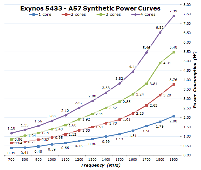
As mentioned in the quote, the A76 (in the Kirin 980) is capable of 2.14W, and the standard configuration is 4 ARM A76, 2 at 2.6 GHz and 2 at 1.92 GHz, along with 4 A55 cores. The Comparion, the Exynos 5433 (see below), has a setup of 4 A57 cores and 4 A53 cores, but the test results shown below try to isolate the A57s as much as possible, keeping the A53s as idle as possible. This is not completely possible in practice, but it gives us a decent idea.Anandtech said: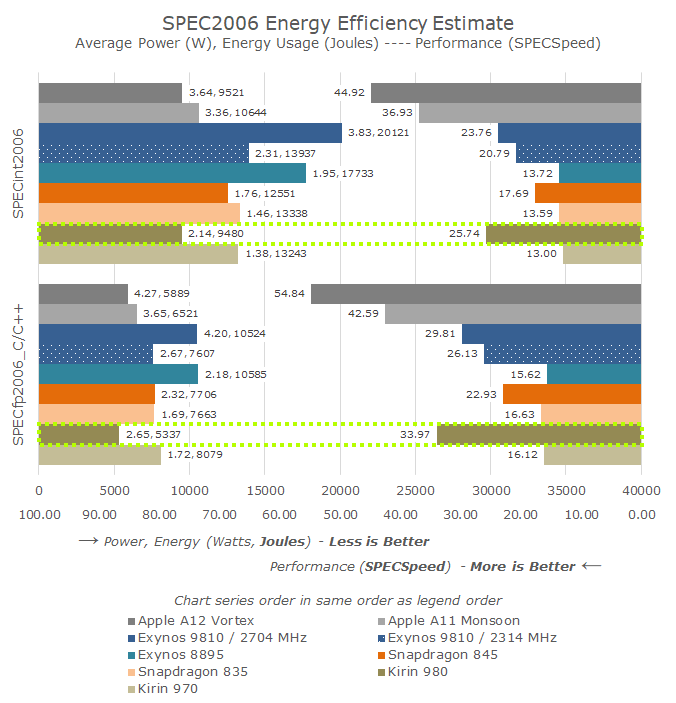
Looking at the SPEC efficiency results, they seem more than validate Arm's claims. As I had mentioned before, I had made performance and power projections based on Arm's figures back in May, and the actual results beat these figures. Because the Cortex A76 beat the IPC projections, it was able to achieve the target performance points at a more efficient frequency point than my 3GHz estimate back then.
The results for the chip are just excellent: The Kirin 980 beats the Snapdragon 845 in performance by 45-48%, all whilst using 25-30% less energy to complete the workloads. If we were to clock down the Kirin 980 or actually measure the energy efficiency of the lower clocked 1.9GHz A76 pairs in order to match the performance point of the S845, I can very easily see the Kirin 980 using less than half the energy.
Tensor cores aren't required, as Control shown, but the implementation wasn't great as the artifacting was immense.So, is it really a must to have tensor cores or whatever in the hardware or can these kind of tech already be applied in the dev stage going from machine learning > machine taught when the game is out?
Nope. I mean devs can try creating assets than can be upscaled better by some specific AI based algorithms, but it wont prevent upscaling in other machines, just quality could be worse.Question:
So this stuff looks impressive and it feels that from here it can only get better. It seems so that up scaling tech like this can save bandwidth etc to achieve an almost identical image quality (depending on the difference)
my question is, isn't this something that is/can be applied in the development stage?
for example, let say X developer is making a game and during development they use machine learning to teach how the output should look like.
Like they have two samples already, one at 720p (which is what the one they want to use because of bandwidth, other resources etc) and one at 1440 (or the desired output). So by using machine learning in this stage, the game engine is "taught" how/what to upscale and how it should look like (because it has already seen a reference image of how it is supposed to look like at native 1440)
the final version is a game that has "all" the benefits of being 720p but looks like 1440 (or whatever was the desired). And with all the extra resources being freed up, perhaps this can go towards Raytracing or whatever..
So, is it really a must to have tensor cores or whatever in the hardware or can these kind of tech already be applied in the dev stage going from machine learning > machine taught when the game is out?
(obviously I'm no dev, just curious to see how these stuff works. feels like it boils down to algorithms and processing power and if it can be done already in the development phase. Perhaps it is already like this.. but like I said, I'm No developer)
The Jaguar in PS4 ane Xbox One was always bad in my opinion... Too weak. I think everyone expected more after 8 years of Xbox 360 when the One launched :)
Jaguars were 1,6ghz vs 3.5ghz in current gen consoles and they could only use 6,5 cores in their work, where next gen will probably can use 7,5, thats 2,5x difference right there. Next gen consoles have multithreading and thats like 50-60% speed-up, so 2.5 * 1,5 = 3,75x.
Not to be a downer - but do you think Nintendo would use "the latest and greatest" technology? They have been utilising something that is generations old each time since the Wii - 14 years of purposefully not targetting the latest technology.The ARM CPU in the Switch is built on planar 20nm, is the very inefficient 4 A57 cores at just 1GHz and uses 1.8 watts. The jump to just 4 A73 cores at 1.5GHz offers twice the performance at 1.1 watts. Moving to 4 A76 at 2GHz offers twice the performance again around that same wattage on 10nm. Hercules actually should offer about 6x the performance of the current Switch CPU per core and come in at half the power consumption. That means you could get 8 cores with less power consumption than the launch Switch, and you can add 4 A55 cores all around 2 watts of power consumption.
The rough napkin math I have is 8 A78 cores @ 2.4GHz + 4 A55 cores @ 2GHz should use less than 2 watts, especially if we are talking about a 5nm 2023 Switch 2. I'd also use 2 of the A55 cores for the OS and offer developers 2 A55 cores @ 2GHz, which is about 33% faster than 2 A57 cores in the launch Switch. You could also down clock those A55 cores to 1.5GHz for Switch gen 1 games and give the device 10+ hours of battery life while playing Zelda.
Combined with DLSS 2.0, Switch 2 will handle next gen far better than the current Switch handles current gen.
We are talking about 3 year old tech by 2023 at least. Switch was originally coming out holiday 2016 with a 20nm 2 Billion transistor SoC, just 2 years after Apple's 20nm 2 Billion transistor A8 SoC. Not talking about new tech here at all. In 3 years we are projected to be using 3nm process node with well over 20 Billion transistors on 100mm^2.Not to be a downer - but do you think Nintendo would use "the latest and greatest" technology? They have been utilising something that is generations old each time since the Wii - 14 years of purposefully not targetting the latest technology.
Yeah, all those people hoping for DLSS, 4k, HDR or SSD for Switch 2 are likely will be disappointed..Not to be a downer - but do you think Nintendo would use "the latest and greatest" technology? They have been utilising something that is generations old each time since the Wii - 14 years of purposefully not targetting the latest technology.
The X1 was the latest and greatest from Nvidia though, the X2 wasnt even out for Partners till after the Switch launched.Not to be a downer - but do you think Nintendo would use "the latest and greatest" technology? They have been utilising something that is generations old each time since the Wii - 14 years of purposefully not targetting the latest technology.
I would love for history to vindicate your view - but i think it helps to be a bit unexpectant of next gen hardware always. Especially if the company making it errs on the side of producing products based on their manufacturing price and mark-up.We are talking about 3 year old tech by 2023 at least. Switch was originally coming out holiday 2016 with a 20nm 2 Billion transistor SoC, just 2 years after Apple's 20nm 2 Billion transistor A8 SoC. Not talking about new tech here at all. In 3 years we are projected to be using 3nm process node with well over 20 Billion transistors on 100mm^2.
The production timelines could have definitely made it so X2 was in the switch. I mean, consoles have debuted new archs throughout their history.The X1 was the latest and greatest from Nvidia though, the X2 wasnt even out for Partners till after the Switch launched.
DLSS is actually a given as all new mobile GPUs from Nvidia have Tensor Cores.Yeah, all those people hoping for DLSS, 4k, HDR or SSD for Switch 2 are likely will be disappointed..
Honestly, people said the same thing with Switch speculation, tech heads in NX threads on the old site were talking about ARM A15 CPU cores, even A12 was being thrown around with head nods. Nintendo uses withered technology, but if you look a bit deeper into the Wii U, you'll see that because of their goals of using a 1990's processor and keeping T1SRAM (forcing the manufacturing on NEC) had more to do with Nintendo's lack of performance on Wii U, than just 'well it's Nintendo'. In fact, we had someone who is an expert on Die shots, speculate that the MCM used on the Wii U must have cost Nintendo over $110 to manufacture. Meanwhile we also know that Nvidia's deal with Nintendo, broke down to ~$55 per Tegra X1 SoC costs, thanks to their financial reports. The reason this is important IMO, is because Wii U actually cost Nintendo more to make than Switch, it was even known at launch that each unit sold for a loss at both $299 and $349 models. With Switch having never sold for a loss as far as we know.I would love for history to vindicate your view - but i think it helps to be a bit unexpectant of next gen hardware always. Especially if the company making it errs on the side of producing products based on their manufacturing price and mark-up.
Thanks for the post, that's very interesting stuff! From DF stuff, I believe they cited the multithreading advantage at around 30%, rather than 50%-60%. Computing with that number, we'd get a bump of:Jaguars were 1,6ghz vs 3.5ghz in current gen consoles and they could only use 6,5 cores in their work, where next gen will probably can use 7,5, thats 2,5x difference right there. Next gen consoles have multithreading and thats like 50-60% speed-up, so 2.5 * 1,5 = 3,75x.
With how the IPC of Zen3 is better like 1,7-2.3x better than Jaguars based on below post => 3,75 * 1,7 = 6,325 or 3,75 * 2,3 = 8,625x . Thats of course fully theoretical, but even reducing this by 20% gives you at least 5x performance boost, which can be greater.
r/Amd - What's the difference in IPC between jaguar and zen/zen+?
4 votes and 10 comments so far on Redditwww.reddit.com
Remember that Switch CPU was already like at least 2x slower than jaguars.
Well, with the Switch 1, the CPU technology as well as the process node went to market in 2014. That's a similar timeline as we would have with the A78 (coming out in 2020 DV) for a Switch 2 in 2023.Not to be a downer - but do you think Nintendo would use "the latest and greatest" technology? They have been utilising something that is generations old each time since the Wii - 14 years of purposefully not targetting the latest technology.
That's true: the PS5/XSX are an example of debuting new tech (or at least launching alongside it). But the speculated specs above don't really fit that bill imo: we are looking at tech that will be 2.5-3 years old by the time the Switch 2 is speculated to launch, whereas Parker was only unveiled in 2016, so a year before the Switch 1 launched. It gives a bit of breathing room for NVIDIA and Nintendo to use some older tech and still meet the specs speculated in my (and others') posts.The production timelines could have definitely made it so X2 was in the switch. I mean, consoles have debuted new archs throughout their history.
I am positive the reason for the switch's hardware is very much related to the idea that NV had a bunch of HW
Your post had better math, mine was estimated on the fly. I'd suggest 2 to 2.5 watt CPU budget for Switch 2, DLSS should save some breathing room for portable clocks on the GPU side, something like 1280 cuda cores (as I've suggested in the past) @ just 614MHz would give almost 1.6TFLOPs of performance, and if you are rendering 540p and upscaling to 1080p on a 7inch screen, you'd have plenty of room there.Still a massive effective bump for sure! Switch 2 probably needs to have more than the 4 cores, as z0m3le suggested for a 2W performance level (but since deleted?). For that, the A78s and the 5nm process are probably required. The math on the A78 is still speculative since we don't have exact performance numbers yet, but perhaps Z0m3le has some idea about the math for an 8-core A78 setup?
Nvidia was tied into a contract with TSMC to purchase a bunch of 20nm chips, Nintendo was the solution, and Nintendo got them at about half the price of Wii U's MCM, so really great deal.
Nvidia was tied into a contract with TSMC to purchase a bunch of 20nm chips, Nintendo was the solution, and Nintendo got them at about half the price of Wii U's MCM, so really great deal.
Nintendo could have very easily gone with the Tegra K1 processor. It was a 2014 release, Nintendo was targeting 2016 and they could have shrunk it to fit 20nm. The real issue with going with 16nm at the time was Nvidia's deal with TSMC forced a very low price for Switch's SoC on 20nm. Nintendo did look into 16nm and just thought it would cost too much. Mariko would have been the result though, not Parker.The production timelines could have definitely made it so X2 was in the switch. I mean, consoles have debuted new archs throughout their history.
I am positive the reason for the switch's hardware is very much related to the idea that NV had a bunch of HW and a design which did not sell as much as they wanted and Nintendo was happy to grab that up. It was about price.
Semi-Accurate did publicly report it with the initial Nvidia is the NX supplier article. I would suggest that first article is about the most accurate piece of NX reporting we ever got, as the information never changed, though a lot of people don't realize how fluid a lot of stuff behind the scenes really is. People report good info that never comes to light, and that is just how the business works, but yeah Nvidia had to produce around 20 Million 20nm chips, and Mariko started showing up in the firmware around the 20 Million sales mark for Switch.I've heard that, and it makes a lot more sense than accidentally making millions of chips without a buyer, however both parties would know that discounted chips wasn't a long term solution.
Not to be a downer - but do you think Nintendo would use "the latest and greatest" technology? They have been utilising something that is generations old each time since the Wii - 14 years of purposefully not targetting the latest technology.
I do not think I am trolling at all or being flippant. We were talking about CPU foundations and differences.Didn't really expect a lol Nintendo port from someone from Digital Foundry.
Call me idiotic but how do I ensure the best quality ray tracing on 1440p?
as a one-time deal, it makes sense. I figure Nvidia was convinced of the product enough to desire a longer-term relationship. the Switch's success justified that desire. now they have a foot in the door to leverage everything they learned to make a technically proficient mobile chipI've heard that, and it makes a lot more sense than accidentally making millions of chips without a buyer, however both parties would know that discounted chips wasn't a long term solution.
I don't think you are either, but a 1GHz A57 quad core CPU on 20nm will be very very easy to see huge gains (5x or more) on A76/A77/A78 with a process node that is literally 3 or 4 generations newer (20nm to 16nm to 10nm to 7nm to 5nm).I do not think I am trolling at all or being flippant. We were talking about CPU foundations and differences.
I am not talking about GPU features here.
The PS5 and XSX use the 4900HS laptop APU with a 4.3GHz clock, that comes with a 7CU? GPU with 1.5GHz clock and has a TDP of 35W. The CPU isn't using some 30W by its self at 3.5GHz (PS5). It's probably under 10 watts for just the CPU.2023? Oh come :)
Just think about it guys. Current gen consoles started with laptop based CPUs, next gen consoles start with Desktop based CPUs, thats a big difference right there. ARM CPUs are amazing, but not that amazing to achieve 50% performance of 30W Ryzen CPUs with 3-4W :)
Huh, interesting, I always thought XB1X was on 12nm, but it's on 16nm just like the PS4PRO. 16 nm -> 7nm is a 70% reduction in area, though, so wouldn't the corresponding Switch 2 chip be 108 mm² (359 mm² * 0.3 = 107.7 mm²)?I don't think you are either, but a 1GHz A57 quad core CPU on 20nm will be very very easy to see huge gains (5x or more) on A76/A77/A78 with a process node that is literally 3 or 4 generations newer (20nm to 16nm to 10nm to 7nm to 5nm).
Just think of the math here, 80mm^2 even on 7nm should have as many transistors as XB1X (7 Billion), and that is a low ball estimate of the Switch 2 SoC.
High clocks require more room between transistors. Switch won't have 3.5ghz CPUs or 2.23ghz GPUs, so it can pack the transistors closer together. A better way to figure out a Switch 2 SoC on 7nm is actually look at Apple's use of TSMC's 7nm process in their last year's A13 SoC, a 8.5 Billion transistor die on 98mm^2. That is 7 Billion transistors packed in 80mm^2.Huh, interesting, I always thought XB1X was on 12nm, but it's on 16nm just like the PS4PRO. 16 nm -> 7nm is a 70% reduction in area, though, so wouldn't the corresponding Switch 2 chip be 108 mm² (359 mm² * 0.3 = 107.7 mm²)?
Just think of the math here, 80mm^2 even on 7nm should have as many transistors as XB1X (7 Billion),
High clocks require more room between transistors. Switch won't have 3.5ghz CPUs or 2.23ghz GPUs, so it can pack the transistors closer together. A better way to figure out a Switch 2 SoC on 7nm is actually look at Apple's use of TSMC's 7nm process in their last year's A13 SoC, a 8.5 Billion transistor die on 98mm^2. That is 7 Billion transistors packed in 80mm^2.
Well, the Xbox One X had CPU frequencies at 2.23 GHz and GPU frequencies at 1.172 GHz, so quite similar imo to what we might expect from Switch 2 in docked mode. But I agree that it's probably better to look at a 7nm comparison point, and that A13 chip seems to indicate what you mentioned, indeed.High clocks require more room between transistors. Switch won't have 3.5ghz CPUs or 2.23ghz GPUs, so it can pack the transistors closer together. A better way to figure out a Switch 2 SoC on 7nm is actually look at Apple's use of TSMC's 7nm process in their last year's A13 SoC, a 8.5 Billion transistor die on 98mm^2. That is 7 Billion transistors packed in 80mm^2.
I don't think it's a larger chip per se more so than a chip with higher CPU/GPU frequencies. Power draw (and also heat production) increase with the square of frequency, so a lot of extra heat is produced with higher frequencies, requiring more spacing between the transistor to prevent them from melting. A Switch chip would use GPU frequencies of just over 1GHz at most instead of 1.78 GHz, and CPU frequencies of about 2 GHz instead of 3.8 GHz, so that's quite a difference. The same thing holds for the XB1X, which has significantly lower clocks than what the XSX pushes.Is this right when Series X has only twice that @360mm^2?
edit: saw your next post, they are both on new TSMC so is that the reason larger chips have fewer transistors per mm^2?
Of course it has to be. I'm wondering if the gap will be narrower than current gens 2.5x. only time will tell.I havent made any metric for the S2 vs PS5 yet, and I wont until we actually know what the specifications are.
I do imagine that it will be a much narrower gap then a blank "10x" statement, nor do I think multipling tflops difference by other metrics is a good way to define it.
That's certainly one way to read it...Didn't really expect a lol Nintendo post from someone from Digital Foundry.
But it does, actually it does take even more than 30W, it sometimes takes 50W.The PS5 and XSX use the 4900HS laptop APU with a 4.3GHz clock, that comes with a 7CU? GPU with 1.5GHz clock and has a TDP of 35W. The CPU isn't using some 30W by its self at 3.5GHz (PS5). It's probably under 10 watts for just the CPU.

 youtu.be
"The difference in power draw at the wall for these two systems is incredible: the G14 with the 4900HS ran comfortably at around 66W long term, compared to 150W for the power boosted 9880H in our HP Omen 15 test system." Those numbers you are sighting for the G14 laptop is ones for the entire system, not just the CPU.But it does, actually it does take even more than 30W, it sometimes takes 50W.
AMD Ryzen 9 4900HS Review
Mobile computing has become the next big target at AMD with its new series of Ryzen 4000 APUs. Today we have the first retail Ryzen 9 4900HS...www.techspot.com
AMD's most important product ever - Ryzen 9 4900HS
Sign up for Private Internet Access VPN at https://lmg.gg/pialinus2Thanks to Thermal Grizzly for sponsoring today's episode! Buy Thermal Grizzly Conductonaut...
Check out the "Sustained Clocks and More Questions" section where they separate CPU power usage from the rest of the system and monitor while it changes the clock speeds."The difference in power draw at the wall for these two systems is incredible: the G14 with the 4900HS ran comfortably at around 66W long term, compared to 150W for the power boosted 9880H in our HP Omen 15 test system." Those numbers you are sighting for the G14 laptop is ones for the entire system, not just the CPU.
Those numbers are measured at the wall too, which means you are losing around 15% to convert the AC current to DC.

